

HDI PCB High Density Interconnect PCB
Product Description
What is HDI technology?
HDI (High Density Interconnect)
HDI is the abbreviation of High Density Interconnector, which is a kind of (technology) for the production of HDI High Quality PCB Products
Hdi Pcb
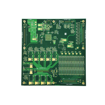
A BVH (buried/blind via hole) PCB with a relatively high line distribution density using micro-blind buried via technology. HDI is a compact product designed for small-capacity users.
HDI PCBs are generally manufactured using a build-up method. The more build-up times, the higher the technical level of the board. Ordinary HDI PCB is basically one-time build-up, high-end HDI uses two or more build-up technology, while adopting advanced PCB technology such as stacking holes, electroplating hole filling, and laser direct drilling.
When the density of the PCB increases beyond the eight-layer board, it is manufactured with HDI, and its cost will be lower than that of the traditional and complex pressing process. HDI High Quality PCB Products are conducive to the use of advanced packaging technology, and its electrical performance and signal accuracy are higher than traditional PCBs. In addition, High Quality PCB Quickturn Products has better improvements in radio frequency interference, electromagnetic wave interference, electrostatic discharge, and heat conduction.


Product Categories : High Frequency Board > Industrial Control PCB